

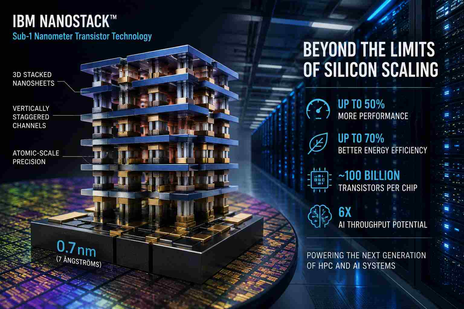
The semiconductor industry has long prioritized smaller transistors, higher chip density, and faster computing. On June 25, IBM unveiled what it describes as the world’s first sub-1-nanometer technology: a 0.7-nanometer (7-angstrom) transistor architecture dubbed "Nanostack." IBM claims this breakthrough offers up to 50 percent greater performance or 70 percent better energy efficiency than its 2021-era 2-nanometer technology, potentially cramming nearly 100 billion transistors onto a fingernail-sized chip. While the announcement has generated significant excitement regarding this long-awaited milestone in silicon scaling, a critical question remains: Does this represent the future of commercial computing, or is it merely an impressive laboratory demonstration destined to remain out of reach for mass production?
The end of traditional scaling
The significance of IBM’s announcement lies not in the transistor dimensions themselves but in how the company achieved them. For years, the semiconductor industry has relied on shrinking transistor features to improve performance and efficiency. However, as dimensions approach atomic scales, traditional methods become increasingly difficult. Leakage currents, quantum effects, manufacturing tolerances, and escalating fabrication costs have made each successive node dramatically harder to commercialize.
IBM’s answer is a three-dimensional architecture called Nanostack. Rather than continuing to flatten more transistors onto a two-dimensional surface, the company vertically stacks and staggers transistor structures, effectively extending Moore’s Law into the third dimension. IBM describes the technology as the industry’s first known three-dimensional nanosheet-based transistor design. From a research perspective, this is a meaningful accomplishment. From a manufacturing perspective, it raises entirely new challenges.
The supercomputing angle
If IBM’s projections prove accurate, the implications for high-performance computing could be substantial. Modern AI training systems consume enormous amounts of electricity and require massive accelerator clusters. Every percentage gain in energy efficiency translates directly into lower operating costs and higher computational throughput. IBM researchers estimate that AI accelerators built with 7-angstrom technology could achieve approximately six times the computational throughput of today’s leading accelerators, potentially reducing large language model training times from months to weeks.
For exaflops supercomputers and hyperscale AI data centers, those gains would be transformative. The challenge is that projected performance gains inside a laboratory environment rarely translate directly into production systems. Memory bottlenecks, packaging constraints, thermal limitations, interconnect overhead, and software inefficiencies frequently erode theoretical advantages. The history of computing is filled with architectures that looked revolutionary on paper but delivered far less dramatic gains in deployed systems.
IBM’s manufacturing problem
Perhaps the biggest reason for skepticism is that IBM no longer manufactures leading-edge semiconductors. The company sold its microelectronics manufacturing business more than a decade ago and now operates primarily as a semiconductor research organization. Its business model depends on licensing technology to foundries rather than producing chips itself. That distinction matters. Creating a laboratory prototype is difficult. Producing millions of chips with acceptable yields, manageable defect rates, and commercially viable costs is exponentially harder.
IBM projects commercial deployment could occur within five years. The semiconductor industry has heard similar timelines before. The company’s 2-nanometer technology, unveiled in 2021, demonstrated IBM’s research capabilities, but it required years of ecosystem development before broader industry adoption became realistic. The same pattern may repeat with Nanostack. The technology’s success ultimately depends on whether foundries such as Samsung, Rapidus, Intel, or others determine that manufacturing complexity and economics justify deployment.
The AI gold rush factor
There is another reason to view the announcement cautiously. The semiconductor industry is currently experiencing unprecedented demand driven by artificial intelligence. Every major chipmaker is under pressure to demonstrate a roadmap that extends beyond current process technologies. As a result, announcements increasingly emphasize future potential rather than near-term products. IBM’s presentation heavily highlights AI, cloud infrastructure, and next-generation computing as beneficiaries of the technology. While those applications are plausible, they remain projections rather than demonstrated commercial outcomes. Investors and technology buyers should remember that the chip unveiled this week is a research platform, not a product roadmap.
Why this still matters
Skepticism should not be confused with dismissal. IBM deserves credit for advancing semiconductor science at a moment when many experts have questioned how much further silicon scaling can realistically proceed. The Nanostack architecture addresses one of the industry’s most pressing challenges: how to continue increasing transistor density when conventional scaling approaches are nearing their physical limits. Whether or not the exact 0.7 nm implementation reaches production, the architectural concepts behind it could influence future generations of processors, AI accelerators, and supercomputing hardware. In that sense, the announcement may prove more important as a blueprint for future semiconductor design than as a specific manufacturing node.
The bottom line
IBM’s sub-1 nanometer chip technology represents a significant research achievement and offers an intriguing glimpse into the future of semiconductor design. The company’s Nanostack architecture demonstrates that innovation in transistor structures continues even as traditional scaling approaches their limits.
But history urges caution. The semiconductor graveyard is littered with breakthrough prototypes that never became commercially viable products. Until major foundries demonstrate manufacturable processes, competitive yields, and sustainable economics, IBM’s 0.7 nm technology remains exactly what it is today: A fascinating laboratory success. Whether it becomes the foundation of the next decade of supercomputing, or merely a milestone on the road toward some entirely different architecture, remains an open question.