

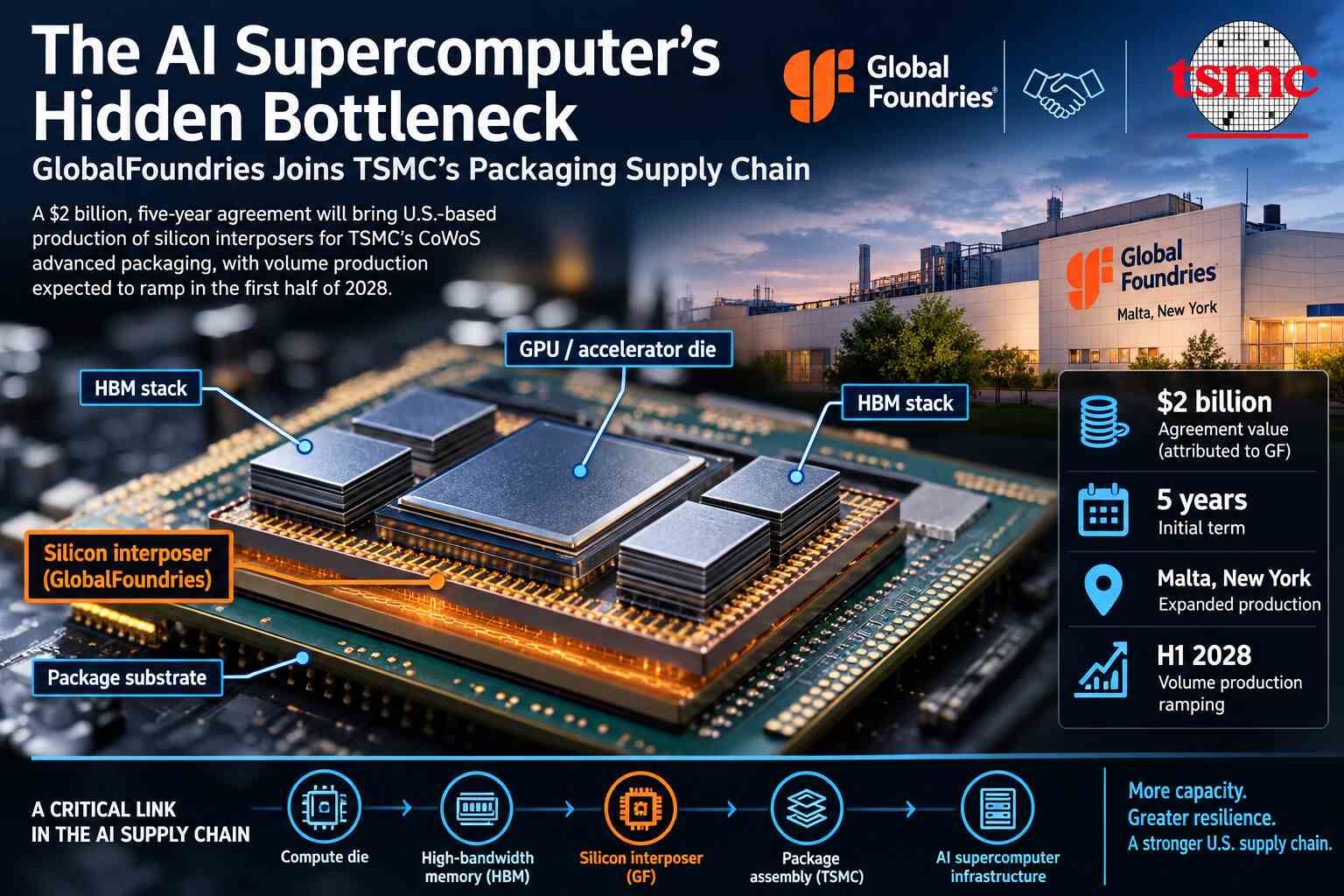
A five-year agreement valued by GlobalFoundries at $2 billion could strengthen U.S. semiconductor manufacturing. Still, a 2028 production ramp leaves a critical question unanswered: how much additional AI computing capacity will it actually unlock?
The race to develop increasingly powerful artificial intelligence supercomputers presents significant manufacturing challenges that extend beyond processor development. As accelerators become more complex and dependent on sophisticated memory systems, the interconnectivity of these components within a single package has emerged as a critical bottleneck for AI infrastructure.
To address this, GlobalFoundries and TSMC have entered into a five-year, $2 billion manufacturing agreement aimed at establishing a U.S.-based supply of silicon interposers for TSMC’s Chip-on-Wafer-on-Substrate (CoWoS) advanced-packaging ecosystem. While GlobalFoundries plans to expand its facility in Malta, New York, with volume production expected by the first half of 2028, the immediate impact of this partnership remains uncertain.
Because production is still years away and specific details regarding output and technical implementation remain undisclosed, it is unclear to what extent this agreement will alleviate supply constraints, increase memory bandwidth, or facilitate the production of finished AI accelerators. Ultimately, the industry must determine whether this additional capacity will sufficiently resolve the physical and electrical integration challenges currently facing large-scale AI workloads.
The bottleneck beneath the processor
The performance of a modern AI accelerator is defined by more than the raw computational throughput of its processing die.
Large-scale AI models necessitate the rapid exchange of vast quantities of data with high-bandwidth memory (HBM). Whether training models across thousands of accelerators or managing data movement within inference systems, the efficiency of data transfer is as consequential as the arithmetic performed by the processors.
Advanced packaging enables these systems by integrating multiple semiconductor dies and memory stacks into a compact assembly with high-density electrical interconnects. In a conventional CoWoS-S configuration, a silicon interposer serves as the vital foundation beneath the logic and HBM stacks, providing the fine-pitch wiring necessary for integration. While the interposer does not perform calculations, it provides the essential physical fabric that facilitates processor-memory synergy.
For supercomputing engineers, this distinction is paramount: theoretical computing capacity is only realized when execution units are supported by sufficient bandwidth and minimal latency. Consequently, the physical integration of logic and memory is a critical pillar of system architecture.
Manufacturing these assemblies at scale presents significant challenges, ranging from precise fabrication and fine-pitch interconnects to maintaining high yields during the integration of expensive components. As GlobalFoundries enters the supply chain at the interposer-manufacturing level, its efforts may alleviate specific component shortages. However, it is important to note that this agreement does not, in isolation, determine the final output volume of finished AI processors from TSMC.
Why TSMC is turning to another foundry
The arrangement illustrates an important feature of the modern semiconductor industry: even leading manufacturers increasingly depend on specialized partners to expand the capacity of complex production ecosystems.
TSMC remains the central packaging integrator in this arrangement. GlobalFoundries will provide manufacturing services for interposers built for TSMC’s CoWoS ecosystem, using technology governed by the companies’ licensing relationship, according to reporting on the agreement.
This is not a second, independent CoWoS platform, nor does it mean GlobalFoundries will manufacture the complete AI accelerators that emerge from TSMC’s packaging lines.
Instead, TSMC gains another manufacturing source for a component used in its broader production process. Externalizing part of that manufacturing could give TSMC additional flexibility as demand grows, while allowing GlobalFoundries to participate in the AI market without needing to manufacture the leading-edge logic dies at the center of those systems.
For GlobalFoundries, the agreement represents an opportunity to extend its role in semiconductor manufacturing beyond its established process-technology markets. The company has been developing differentiated capabilities in areas including silicon photonics and specialized semiconductor manufacturing. The interposer agreement adds another potential source of business tied to AI infrastructure.
Yet the commercial relationship also creates a dependency. TSMC controls the packaging ecosystem into which the components must fit. GlobalFoundries’ ability to benefit will depend on the requirements of TSMC and its customers, the economics of manufacturing the components, and the volume ultimately assigned to its facility.
The agreement establishes a route into the market. It does not yet reveal how profitable that route will be.
The $2 billion headline needs context
The announced value is substantial enough to attract attention, but it requires careful interpretation.
GlobalFoundries describes the arrangement as a $2 billion agreement with an initial term of five years. Dividing that figure evenly across five years produces a simple average of $400 million annually. That is an arithmetic illustration, not a disclosed revenue schedule.
The companies have not publicly specified whether the entire amount represents firm purchase commitments, expected manufacturing revenue, or another commercial measure of the agreement’s value. They have also not disclosed the capital expenditure required for the Malta expansion or a detailed production ramp.
Those omissions matter.
A manufacturing agreement valued at $2 billion does not necessarily mean that $2 billion will be paid immediately, that all the revenue is guaranteed, or that GlobalFoundries will recognize an even $400 million each year. Revenue would depend on the agreement’s terms, production timing, customer demand, and the delivery of qualifying components.
The figure should therefore be understood as the value GlobalFoundries has assigned to the agreement, rather than as a confirmed $2 billion investment by TSMC or an unconditional purchase order.
The timing adds another qualification. GlobalFoundries expects volume production to begin ramping in the first half of 2028. Capacity must be installed, manufacturing processes qualified, and output brought to commercially useful levels. The announcement does not disclose the expected production rate or the time required to reach full capacity.
The financial opportunity is real enough to merit attention. Its ultimate size and profitability, however, remain unproven.
The critical technical question: Which CoWoS architecture?
One of the most consequential unanswered questions concerns the specific interposer technology GlobalFoundries will manufacture.
CoWoS is a family of advanced-packaging approaches, not a single, interchangeable product. The distinction between its architectures affects how the interposer is built, how components are integrated, and which processor designs can use the resulting package.
CoWoS-S uses a full silicon interposer. CoWoS-L uses a different approach involving redistribution layers and localized silicon interconnect structures. These approaches have different manufacturing requirements and design implications.
GlobalFoundries’ announcement identifies silicon interposers and embedded deep-trench capacitor components, but it does not clearly specify the exact CoWoS variant, the complete component mix, or the accelerator designs that will use the Malta output.
That gap limits any attempt to calculate the agreement’s effect on the supply of leading AI processors.
If the new production line primarily supports one packaging architecture, its value will depend partly on the demand outlook for that architecture and the designs that use it. If the output supports another configuration or a wider set of components, the potential market and manufacturing economics could differ.
The question is especially relevant as the industry evolves toward more complex multi-die packages and increasingly demanding memory configurations. Manufacturing capacity must match the package designs customers actually need, not simply a broad category of advanced semiconductor components.
Without confirmation from GlobalFoundries or TSMC, assigning the new capacity to specific GPU generations or accelerator programs would be speculative.
For HPC engineers, this is more than a technical footnote. The interposer’s characteristics, the package architecture, the memory configuration, and the completed assembly all affect the system that ultimately reaches a data center.
Deep-trench capacitors and power delivery
GlobalFoundries has specifically highlighted embedded deep-trench capacitor components as part of the advanced-packaging technology associated with the project.
These structures can provide capacitance within silicon, helping stabilize local power delivery. When a high-performance processor switches rapidly between computational states, its power-delivery network must respond to changing current demands while maintaining supply voltage within acceptable limits.
Power integrity becomes more challenging as packages integrate high-power compute dies and multiple HBM stacks into increasingly dense assemblies. Voltage fluctuations can affect reliable operation, and the placement and characteristics of decoupling capacitance are important elements of package and power-delivery design.
Embedding capacitors in silicon can provide a way to place capacitance close to the circuitry it supports. However, the actual benefits depend on the implementation, electrical design, package geometry, and operating conditions.
The announcement does not quantify the electrical or performance improvements associated with the components GlobalFoundries will produce. It would therefore be premature to claim that the agreement will directly increase accelerator performance or reduce power consumption by a particular amount.
The more defensible conclusion is that the project addresses a component of the increasingly sophisticated electrical and physical integration required by next-generation AI packages.
A U.S. supply chain, but not yet a domestic AI chip ecosystem
The Malta expansion also has a geographic dimension.
GlobalFoundries says the agreement will establish the first U.S.-based source of silicon interposers supporting advanced-packaging technologies of the type described in its announcement. That is a company claim and should be attributed as such until independently established in its precise scope.
The strategic rationale is clear. Semiconductor production is distributed across a global network of fabrication plants, packaging facilities, memory manufacturers, substrate suppliers, and equipment vendors. Concentration of critical capabilities in particular regions can create exposure to geopolitical disruption, transportation constraints, and sudden changes in demand.
Adding a U.S.-based source for an important packaging component could give TSMC and its customers another option. It may also complement broader efforts to develop semiconductor manufacturing and packaging capabilities within the United States.
But a domestic interposer supply does not, by itself, create a fully domestic AI accelerator supply chain.
A finished AI package still depends on logic dies, HBM, package substrates, precision assembly, testing, and other inputs. The geographic origin of each component and the location of each manufacturing step determine how much of the supply chain is actually domestic.
Nor have the companies confirmed where GlobalFoundries’ interposers will ultimately be used. A New York manufacturing source could potentially support packaging operations in the United States or elsewhere, but the agreement does not establish the destinations of the components.
That distinction is essential when evaluating claims about supply-chain resilience. Manufacturing one critical component domestically can reduce a specific dependency. It does not eliminate the wider dependencies surrounding the finished system.
The 2028 problem: What happens before the capacity arrives?
The production timetable is the most immediate limitation on the deal’s near-term significance.
The agreement was announced in October 2026, with volume production expected to begin ramping during the first half of 2028. That schedule positions the project to contribute to a future phase of AI infrastructure expansion rather than providing an immediate solution to current supply constraints.
Even after the initial ramp begins, actual contributions will depend on production yields, installed capacity, customer qualification, and the availability of complementary packaging and assembly resources.
The distinction between component capacity and finished-system output is crucial. Increasing interposer production will not automatically increase the number of operational accelerators if other stages of the manufacturing process remain constrained.
For data-center operators and supercomputer builders, the metric that ultimately matters is not the number of interposers produced in isolation. It is the number of qualified, fully assembled accelerators that can be delivered, integrated, powered, cooled, and operated reliably.
The GlobalFoundries agreement could help support that outcome, but the public information does not yet allow its contribution to be quantified.
What the agreement does not tell us
Several missing details will determine whether this becomes a meaningful expansion of AI manufacturing capacity or a strategically useful but relatively limited addition to the supply chain.
First, the companies have not disclosed the planned production capacity, measured in interposers or wafers over a defined period. Without those figures, it is impossible to estimate the share of TSMC’s requirements that Malta might eventually supply.
Second, the manufacturing investment remains undisclosed. The equipment, process qualification, facility modifications, and production ramp required to support the agreement will influence the economics and timing of the project.
Third, the precise product specifications and packaging architectures have not been fully established in the public announcement. Those details are necessary to evaluate the addressable market and the agreement’s potential durability.
Fourth, the commercial terms remain insufficiently detailed to determine how the $2 billion is structured or how much revenue GlobalFoundries can reasonably expect to recognize over the agreement’s life.
Finally, the relationship between this interposer supply and other U.S. packaging initiatives remains an open question. The agreement could eventually complement packaging operations in Arizona, but neither company has established that the Malta output will feed a particular U.S. packaging facility.
These are not reasons to dismiss the deal. They are the questions that separate a strategic announcement from a measurable change in the industry’s ability to manufacture AI hardware.
The bigger lesson for supercomputing
The GlobalFoundries–TSMC agreement illustrates how the constraints on AI infrastructure are becoming more distributed across the semiconductor manufacturing process.
For years, discussions of advanced computing hardware have concentrated heavily on processor performance, transistor scaling, and accelerator counts. Those remain important, but the economics and availability of large AI systems increasingly depend on the integration of compute, memory, power delivery, packaging, and the manufacturing processes connecting them.
Advanced packaging is a particularly important part of that equation because it determines how effectively multiple dies and memory stacks can be assembled into a functioning system. As accelerator designs become more complex, the supply of specialized packaging components becomes part of the broader capacity planning problem.
The same lesson applies at the data-center level. More accelerator capacity is useful only when the surrounding infrastructure can support it. Power availability, cooling, networking, storage, and operational reliability all influence how much computing performance an organization can deploy in practice.
The semiconductor supply chain has its own version of this constraint: a shortage in one specialized manufacturing stage can limit the output of an otherwise capable production network.
GlobalFoundries is positioning itself to mitigate these constraints; its agreement with TSMC could enhance supply chain flexibility and bolster the U.S. manufacturing infrastructure for critical packaging components.
However, the ultimate significance of this announcement will be defined by actual production volumes, technical specifications, commercial terms, and the resulting increase in finished package output. The evolution of AI supercomputing is no longer solely a competition to design the fastest processor; it has become a complex challenge of manufacturing, interconnecting, powering, and delivering the holistic ecosystem required to scale those processors effectively.
While GlobalFoundries and TSMC have initiated a meaningful expansion of this manufacturing base, the critical test remains whether the additional capacity is delivered on schedule, aligns with evolving packaging architectures, and produces a measurable impact on the supply of completed AI computing systems. Until further details are disclosed, this $2 billion agreement should be viewed as a strategically significant investment in the future of high-performance computing, rather than an immediate solution to current industry bottlenecks.