

 How to resolve AdBlock issue?
  We breathe to survive. But a breath of fresh air does more than fill our lungs. New research from Aarhus University the second largest and second oldest university in Denmark, indicates that breathing impacts our emotions, attention and how we can process the outside world.
“Breathe in… Breathe out…” Or: “take a deep breath and count to ten.” The calming effect of breathing in stressful situations, is a concept most of us have met before. Now Professor Micah Allen from the Department of Clinical Medicine at Aarhus University has come to a step closer to understanding how the very act of breathing shapes our brain.
The researchers synthesized results from more than a dozen studies with rodent, monkey, and human brain imaging, and used it to propose a new computational model that explains how our breathing influences the brain’s expectations.
“What we found is that, across many different types of tasks and animals, brain rhythms are closely tied to the rhythm of our breath. We are more sensitive to the outside world when we are breathing in, whereas the brain tunes out more when we breathe out. This also aligns with how some extreme sports use breathing, for example, professional marksmen are trained to pull the trigger at the end of exhalation,” explains Professor Micah Allen.
The study suggests that breathing is more than just something we do to stay alive, explains Micah Allen.
“It suggests that the brain and breathing are closely intertwined in a way that goes far beyond survival, to actually impact our emotions, our attention, and how we process the outside world. Our model suggests there is a common mechanism in the brain which links the rhythm of breathing to these events.”
Breathing can affect our mental health
Understanding how breathing shapes our brain, and by extension, our mood, thoughts, and behaviors, is an important goal in order to better prevent and treat mental illness.
“Difficulty breathing is associated with a very large increase in the risk for mood disorders such as anxiety and depression. We know that respiration, respiratory illness, and psychiatric disorders are closely linked. Our study raises the possibility that the next treatments for these disorders might be found in the development of new ways to realign the rhythms of the brain and body, rather than treating either in isolation,” explains Micah Allen.
Stabilizing our mind through breathing is a well-known and used tactic in many traditions such as yoga and meditation. The new study sheds light on how the brain makes it possible. It suggests that there are three pathways in the brain that control this interaction between breathing and brain activity. It also suggests that our pattern of breathing makes the brain more “excitable”, meaning neurons are more likely to fire during certain times of breathing
New research to come
The new study gives researchers a new target for future studies for example persons with respiratory or mood disorders, and Micah Allen and his group already have already started new projects based on the study.
“We have a variety of ongoing projects that are both building on and testing various parts of the model we have proposed. Ph.D. Student Malthe Brændholt is conducting innovative brain imaging studies in humans, to try and understand how different kinds of emotional and visual perception are influenced by breathing in the brain,” says Micah Allen.
The team is also collaborating with the Pulmonology team at Aarhus University Hospital, where tools developed in the lab are used to understand whether a person suffering from long-covid may have disruptions in the breath-brain alignment. And there are more projects coming, says Micah Allen.
”We will be using a combination of human and animal neuroimaging to better understand how breathing influences the brain, and also utilizing exploring how different drugs influence respiratory-brain interaction. We would also like to someday study how lifestyle factors like stress, sleep, and even things like winter swimming influence breath-brain interaction. We are very excited to continue this research,” says Micah Allen.
 Jordi Sort, Enric Menéndez and Zhengwei Tan in the lab at the UAB.") Neuromorphic supercomputing is a new computing paradigm in which the behavior of the brain is emulated by mimicking the main synaptic functions of neurons. Among these functions is neuronal plasticity: the ability to store information or forget it depending on the duration and repetition of the electrical impulses that stimulate neurons. This plasticity would be linked to learning and memory.
Neuromorphic supercomputing is a new computing paradigm in which the behavior of the brain is emulated by mimicking the main synaptic functions of neurons. Among these functions is neuronal plasticity: the ability to store information or forget it depending on the duration and repetition of the electrical impulses that stimulate neurons. This plasticity would be linked to learning and memory.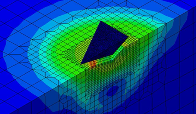 Scientists in Japan have combined two computational models to extract more data on steel alloys from a single test, with implications for the discovery of new materials.